- 您现在的位置:买卖IC网 > Sheet目录687 > EMI4182MTTAG (ON Semiconductor)IC FILTER COMMON MODE ESD 10WDFN
�� �
�
�EMI4182�
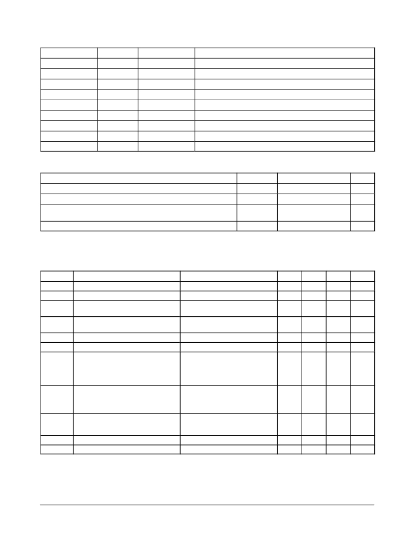
�PIN� FUNCTION� DESCRIPTION�
�Pin� Name�
�In_1+�
�In_1� ?�
�Out_1+�
�Out_1� ?�
�In_2+�
�In_2� ?�
�Out_2+�
�Out_2� ?�
�V� N�
�Pin� No.�
�1�
�2�
�10�
�9�
�4�
�5�
�7�
�6�
�3,� 8�
�Type�
�I/O�
�I/O�
�I/O�
�I/O�
�I/O�
�I/O�
�I/O�
�I/O�
�GND�
�Description�
�CMF� Channel� 1+� to� Connector� (External)�
�CMF� Channel� 1� ?� to� Connector� (External)�
�CMF� Channel� 1+� to� ASIC� (Internal)�
�CMF� Channel� 1� ?� to� ASIC� (Internal)�
�CMF� Channel� 2+� to� Connector� (External)�
�CMF� Channel� 2� ?� to� Connector� (External)�
�CMF� Channel� 2+� to� ASIC� (Internal)�
�CMF� Channel� 2� ?� to� ASIC� (Internal)�
�Ground�
�ABSOLUTE� MAXIMUM� RATINGS� (T� A� =� 25� °� C� unless� otherwise� noted)�
�Parameter�
�Operating� Temperature� Range�
�Storage� Temperature� Range�
�Maximum� Lead� Temperature� for� Soldering� Purposes�
�(1/8”� from� Case� for� 10� seconds)�
�DC� Current� per� Line�
�Symbol�
�T� OP�
�T� STG�
�T� L�
�I� LINE�
�Value�
�?� 40� to� +85�
�?� 65� to� +150�
�260�
�100�
�Unit�
�°� C�
�°� C�
�°� C�
�mA�
�Stresses� exceeding� Maximum� Ratings� may� damage� the� device.� Maximum� Ratings� are� stress� ratings� only.� Functional� operation� above� the�
�Recommended� Operating� Conditions� is� not� implied.� Extended� exposure� to� stresses� above� the� Recommended� Operating� Conditions� may� affect�
�device� reliability.�
�ELECTRICAL� CHARACTERISTICS� (T� A� =� 25� °� C� unless� otherwise� noted)�
�Symbol�
�I� LEAK�
�Parameter�
�Channel� Leakage� Current�
�Test� Conditions�
�T� A� =� 25� °� C,� V� IN� =� 5� V,� GND� =� 0� V�
�Min�
�Typ�
�Max�
�1.0�
�Unit�
�m� A�
�V� F�
�C� IN�
�R� CH�
�f� 3dB�
�F� atten�
�V� ESD�
�V� CL�
�R� DYN�
�V� RWM�
�V� BR�
�Channel� Negative� Voltage�
�Channel� Input� Capacitance� to� Ground�
�(Pins� 1,� 2,� 4,� 5� to� Pins� 3,� 8)�
�Channel� Resistance�
�(Pins� 1� ?� 10,� 2� ?� 9,� 4� ?� 7� and� 5� ?� 6)�
�Differential� Mode� Cut� ?� off� Frequency�
�Common� Mode� Stop� Band� Attenuation�
�In� ?� system� ESD� Withstand� Voltage�
�a)� Contact� discharge� per� IEC� 61000� ?� 4� ?� 2�
�standard,� Level� 4� (External� Pins)�
�b)� Contact� discharge� per� IEC� 61000� ?� 4� ?� 2�
�standard,� Level� 1� (Internal� Pins)�
�TLP� Clamping� Voltage�
�(See� Figure� 12)�
�Dynamic� Resistance�
�Positive� Transients�
�Negative� Transients�
�Reverse� Working� Voltage�
�Breakdown� Voltage�
�T� A� =� 25� °� C,� I� F� =� 10� mA�
�T� A� =� 25� °� C,� At� 1� MHz,� GND� =� 0� V,�
�V� IN� =� 1.65� V�
�50� W� Source� and� Load� Termination�
�@� 800� MHz�
�(Notes� 1� and� 2)�
�Forward� I� PP� =� 8� A�
�Forward� I� PP� =� 16� A�
�Forward� I� PP� =� ?� 8� A�
�Forward� I� PP� =� ?� 16� A�
�T� A� =� 25� °� C,� I� PP� =� 1� A,� t� P� =� 8/20� m� s�
�Any� I/O� pin� to� Ground;�
�Notes� 1� and� 3�
�(Note� 3)�
�I� T� =� 1� mA;� (Note� 4)�
�0.1�
�±� 15�
�±� 2�
�5.6�
�0.8�
�8.0�
�2.0�
�30�
�12�
�18�
�?� 6�
�?� 12�
�1.36�
�0.6�
�1.5�
�1.3�
�5.0�
�9.0�
�V�
�pF�
�W�
�GHz�
�dB�
�kV�
�V�
�V�
�V�
�V�
�V�
�V�
�1.� Standard� IEC61000� ?� 4� ?� 2� with� C� Discharge� =� 150� pF,� R� Discharge� =� 330,� GND� grounded.�
�2.� These� measurements� performed� with� no� external� capacitor.�
�3.� TVS� devices� are� normally� selected� according� to� the� working� peak� reverse� voltage� (V� RWM� ),� which� should� be� equal� to� or� greater� than� the� DC�
�or� continuous� peak� operating� voltage� level.�
�4.� V� BR� is� measured� at� pulse� test� current� I� T� .�
�http://onsemi.com�
�2�
�发布紧急采购,3分钟左右您将得到回复。
相关PDF资料
EMI4183MTTAG
IC FILTER COMMON MODE ESD 16WDFN
EMI4192MTTAG
IC COMMON MODE FILTER ESD 10WDFN
EMI5208MUTAG
IC EMI FILTER 8CH ESD 16UDFN
EMI7206MUTAG
IC EMI FILTER 6CH ESD 12-UDFN
EMI9406MUTAG
IC EMI LC FILTER 6CH 12-UDFN
EMI9408MUTAG
IC EMI LC FILTER 8CH 16-UDFN
ESE-15700
SWITCH SLIDE/PUSH HORZ SMD
EXC-EMT103DT
EXC-EMT/EMI FILTER 10000PF
相关代理商/技术参数
EMI4182MU-D.PDF0
制造商:ONSEMI 制造商全称:ON Semiconductor 功能描述:Common Mode Filter with ESD Protection
EMI4182MUTAG
制造商:ON Semiconductor 功能描述:2PAIR CMF WITH ESD IN UDF - Tape and Reel
EMI4183
制造商:ONSEMI 制造商全称:ON Semiconductor 功能描述:Common Mode Filter with ESD Protection
EMI4183MTTAG
功能描述:电磁干扰滤波器 COMMON MODE FILTER W ESD RoHS:否 制造商:STMicroelectronics 电容:12 pF 电路类型: 最大直流电流: 最大直流电阻: 电压额定值:6 V 容差: 端接类型:SMD/SMT 工作温度范围:- 30 C to + 85 C 系列:EMIF03
EMI4183MU
制造商:ONSEMI 制造商全称:ON Semiconductor 功能描述:Common Mode Filter with ESD Protection
EMI4183MUTAG
制造商:ON Semiconductor 功能描述:3PAIR CMF WITH ESD IN UDF - Tape and Reel 制造商:ON Semiconductor 功能描述:REEL / 3PAIR CMF WITH ESD IN UDF
EMI4184MUTAG
制造商:ON Semiconductor 功能描述:4PAIR CMF WITH ESD - Tape and Reel 制造商:ON Semiconductor 功能描述:REEL / 4PAIR CMF WITH ESD
EMI4192
制造商:ONSEMI 制造商全称:ON Semiconductor 功能描述:Common Mode Filter with ESD Protection